QTE | IMRE

- Featured Publications -
Gate-Defined Quantum Confinement in CVD 2D WS2
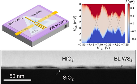
As we continue to squeeze the last few drops from the lemon that is Moore's law, replacement of traditional channel materials and dielectrics are required. Here we focus on 2D tungsten disulfide as the channel and hafnium oxide as a dielectric.
Importantly, we focus on using materials grown with scalable approaches such as chemical vapour deposition (CVD) and atomic layer deposition (ALD). Studies employing such scalable approaches are unfortunately still rare as academia usually favours mechanical exfoliation, otherwise known as the scotch tape technique, followed by layer-by-layer assembly. While such manual assembly techniques can produce materials of the highest quality, the technique is extremely labour intensive and limited in scalability. Flakes produced typically range on micrometre scale and are random in sizes, shapes and positions.
By using our previously developed indium alloy contacts, we can now study such CVD WS2 / ALD HfO2 heterostructures at low temperatures. We clearly isolated the influence of the HfO2 dielectric on carrier transport and showed how interface roughness, a commonly overlooked factor, played a dominant role, rather than charge impurities as had been previously thought. Understanding such low temperature carrier scattering mechanisms is key to the design of increasingly complex devices for quantum applications.
Finally, we demonstrate a gate defined quantum dot in a CVD WS2 / ALD HfO2 heterostructure. The measurements at 20 mK show diamond shaped regions of strongly suppressed conductance. Such oscillating current behaviour is a key signature of effective quantum confinement and a transition to a single-electron tunnelling regime. We estimate a quantum dot size of ~58 nm, several times smaller than other reported devices due to our use of a thin high-k dielectric. While more material development and engineering will be required, the establishment of such TMDC based quantum dot device are a significant step towards their use for quantum information processing applications.
Impact of S-Vacancies on the Charge Injection Barrier at the Electrical Contact with the Molybdenum Disulfide Monolayer

One of the key steps toward integrating 2D semiconducting TMDCs in electronic circuitry is the ability to reduce contact resistance at their interfaces and/or the ability to control the transport of majority charge carriers into devices. At the time of writing, high contact resistance at the interface between semi-metal/metal electrodes and the TMDC surface constituted a major bottleneck toward creating quantum devices of high performance. Amongst other complications, high contact resistances cause heating in the device and not only affect the current flowing through it; they can also compromise its function by destroying fragile quantum states.
To improve the viability of contacts, research has focused on the influence of lattice imperfections on charge transport. The mechanism by which these defects affect transport is still a subject of intense debate.
In our study, we introduced sulfur vacancies into a TMDC monolayer (ML) by utilizing argon gas sputtering. The molybdenum disulfide ML we used was interfaced with a graphitic substrate, and changes to ML energy levels were studied through X-ray photoelectron spectroscopy (XPS) and angular-resolved photoelectron spectroscopy (ARPES) to reveal their electronic properties. We explored the impact of defect density on contact performance and proposed an effective strategy to tailor contacts for TMDC-based quantum devices.
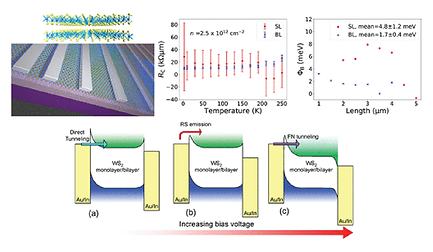
Quantum Transport in Two-Dimensional Tungsten Disulfide with High-Efficiency Carrier Injection through Indium Alloy Contacts
The quantum computer of today requires operating at extremely low temperatures; as low as 100 mK, or -273 degrees Celcius. Such extreme conditions are necessary to preserve the fragile quantum states of these devices.
In our search for novel semiconductor materials that can be used as suitable solid-state qubits, our group focused on two-dimensional tungsten disulfide, an atomically thin transition metal dichalcogenide (TMDC) semiconductor.
The foray into this field, however, was not straightforward. Charge carriers were expected to exhibit higher mobility in tungsten disulfide than its more well-known counterpart molybdenum disulfide due to its lower effective mass. However, less is known about this material, and the lack of high-quality materials and a robust contacting strategy operable at cryogenic temperatures have also hindered quantum transport research in 2D tungsten disulfide.
In our study, we selected an indium alloy for metallic contacts in our devices. We measured contact resistances and metal-semiconductor barrier heights that are among the lowest reported for TMDC contacts.
Thanks to our high quality contacts that worked well at temperatures down to 3 K, we could study quantum transport in single-layered and bilayered devices. Surprisingly, we found that in bilayered devices at low temperatures, carrier transport occurred predominantly in the top metal-contacted layer, while the bottom layer screened the mobile carriers from potential sources of disorder from the substrate. Our experimental findings were further supported by density-functional theory simulation studies, and we gained deeper insights into quantum transport and the properties of the semiconductor-metal interface.
Toward Valley-Coupled Spin Qubits

The power of quantum computing has been realized on a small scale, involving a few tens of qubits. Further upscaling of the quantum computers may require complete revamps of device infrastructure and material platform.
In this publication, we review key advances in the device architecture, material processing, theoretical modelling, and operational strategy of developing scalable quantum devices in 2D transition metal dichalcogenides (TMDCs). We discuss ongoing studies and outstanding challenges in scalable high-quality growth, material characterization, and transport measurements of TMDC based on quantum devices. Finally, we present our perspective on possible exciting future developments for key breakthroughs towards spin-valley qubits.